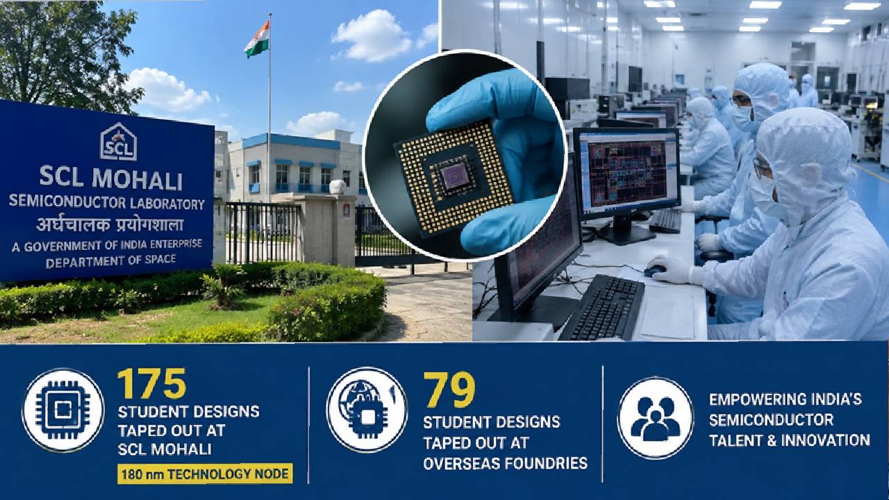
The Semi-Conductor Laboratory (SCL) in Mohali has achieved a significant milestone in India’s semiconductor journey by successfully completing the tape-out of 175 chip designs developed by engineering students using its 180-nanometre (nm) fabrication technology. The achievement marks one of the largest academic chip design exercises undertaken in the country and highlights Mohali’s growing importance in India’s semiconductor ecosystem.
The tape-out process represents the final stage of a chip’s design before it moves into fabrication. Successfully reaching this stage means that the student-developed integrated circuits have passed the required design verification process and are now ready for manufacturing on silicon wafers.
In addition to the 175 chip designs fabricated at SCL Mohali, 79 more chip designs created by Indian students have been taped out at international semiconductor foundries. Together, these achievements reflect the rapid progress being made under India’s efforts to strengthen semiconductor design capabilities and provide students with exposure to industry-level chip development.
The student projects were developed through collaboration between academic institutions, researchers and national semiconductor programmes that aim to build a strong domestic talent pool in Very Large Scale Integration (VLSI) design and semiconductor engineering. By providing access to advanced design software, fabrication facilities and technical mentorship, the initiative enables students to gain practical experience beyond classroom learning.
Located in Sector 72, Mohali, the Semi-Conductor Laboratory is India’s premier government-owned semiconductor fabrication facility and currently operates a 180 nm CMOS technology node. Over the years, the laboratory has supported strategic sectors including space, defence, healthcare, electronics and scientific research while also contributing to indigenous semiconductor development.
Industry experts believe that giving students access to real chip fabrication significantly enhances India’s semiconductor talent pipeline. Designing a chip and seeing it progress to fabrication provides hands-on experience in integrated circuit design, verification and manufacturing processes, helping prepare engineers for careers in one of the world’s fastest-growing technology sectors.
The achievement also aligns with the Government of India’s broader vision of creating a self-reliant semiconductor ecosystem. As the country continues to invest in chip manufacturing, design innovation and electronics production, institutions like SCL Mohali are expected to play a central role in developing skilled manpower and supporting indigenous technology.
The growing participation of universities in chip design programmes reflects increasing interest among students in semiconductor engineering. Educational institutions across the country have been actively encouraging research in areas such as embedded systems, artificial intelligence hardware, communication technologies and Internet of Things (IoT) applications, many of which rely on advanced chip design.
Technology experts say initiatives that connect academia with fabrication facilities help bridge the gap between theoretical education and industrial requirements. Such collaborations not only strengthen research capabilities but also encourage innovation by allowing students to convert their designs into functional semiconductor devices. With India’s semiconductor sector witnessing unprecedented growth, Mohali continues to emerge as a key centre for chip research, design and fabrication. The successful tape-out of 175 student-designed chips at SCL represents another important milestone in the country’s journey towards becoming a globally competitive semiconductor hub while reinforcing Mohali’s position as a leading destination for high-technology innovation.

Mohali Dialogues
I work as a journalist and digital content writer for Mohali Dialogues, specializing in local news, civic issues, government updates, politics, education, business, and technology. I am committed to creating factual, well-researched, and engaging stories that help readers stay informed about the latest developments in Mohali, Punjab, and beyond.
Join the conversation
Keep it useful, respectful and relevant to the story.